
ADI
图片可能具有代表性。
产品详情请参阅规格.
产品详情请参阅规格.
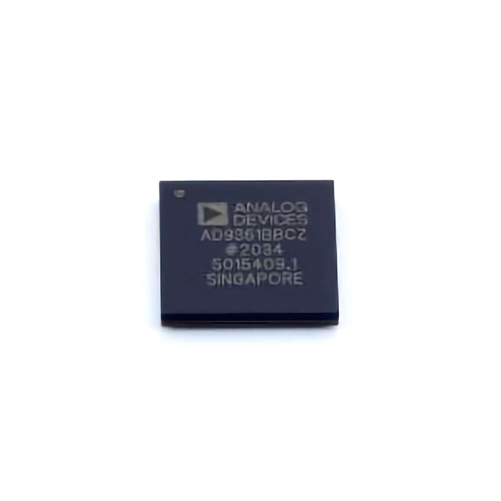
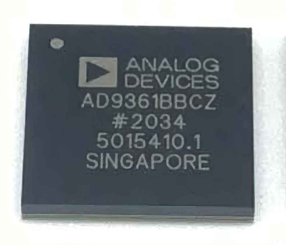
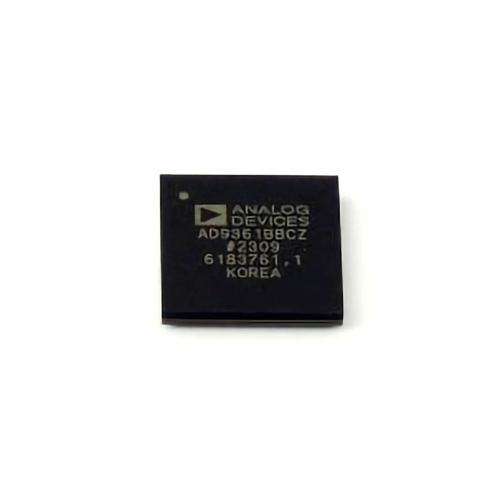
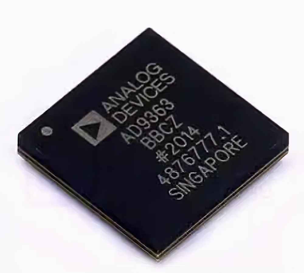
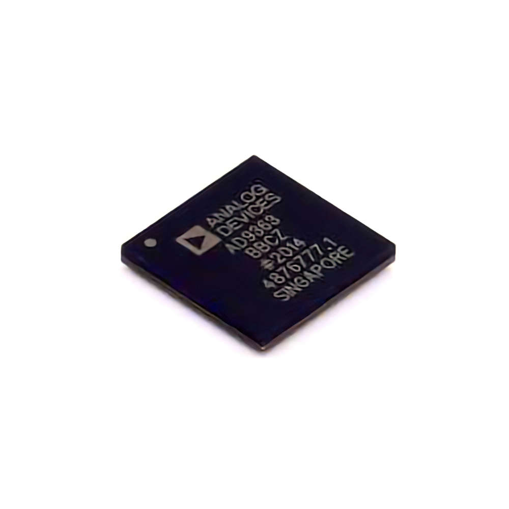
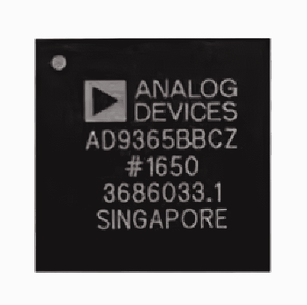
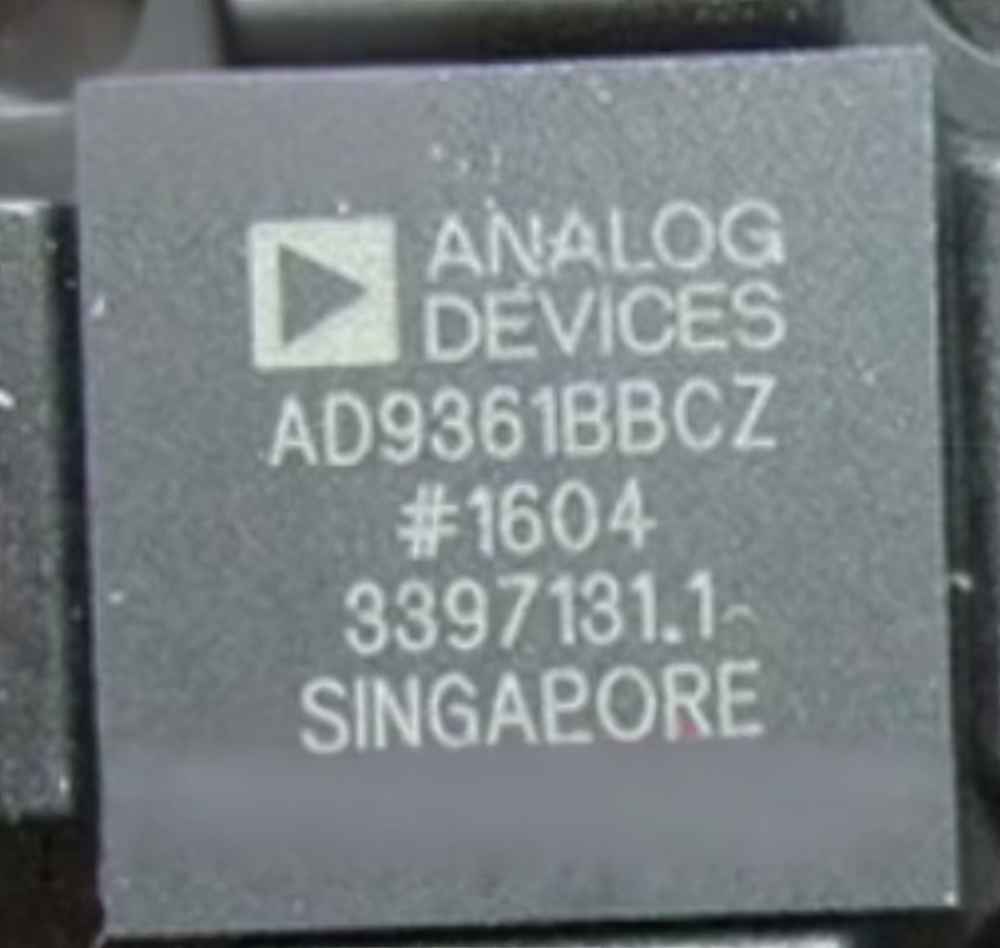
AD9361BBCZ
AD9361BBCZ
型号
AD9361BBCZ
类目
RF Chip/Antenna > Wireless Transceiver Chip
制造商/品牌
ADI
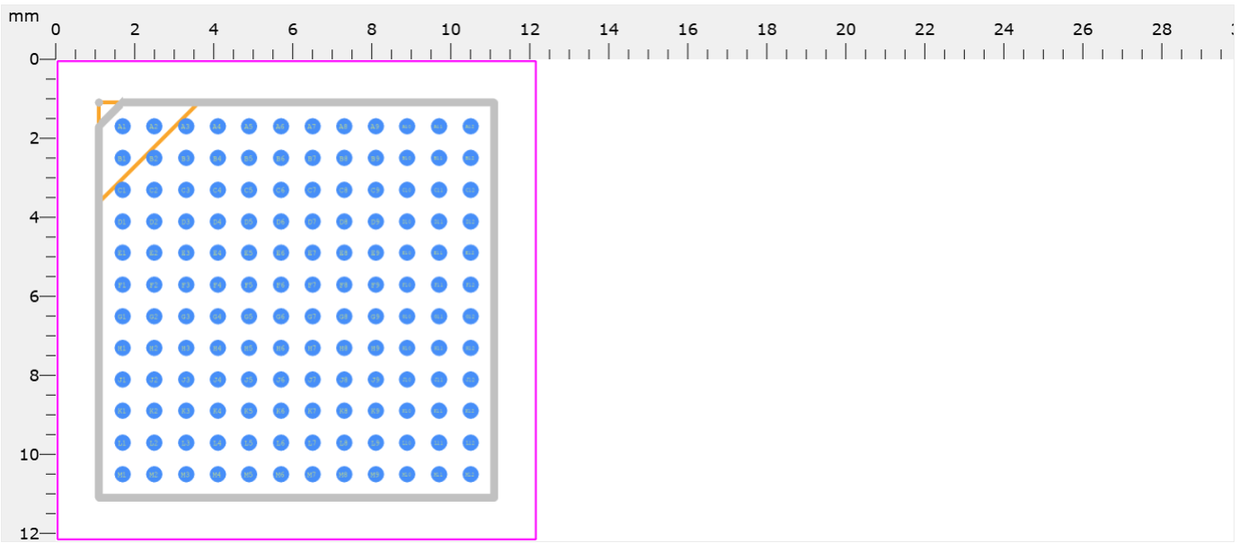
封装
BGA-144
包装
the tray
包裹数量
184
简介
请求报价
请填写所有必填字段并点击“提交”,我们将在12小时内通过电子邮件与您联系。如果您有任何问题,请留言或发送电子邮件至 2762329346@qq.com,我们将尽快回复。
有货 74447 PCS
联系信息
more_pkgimg

more_schimg

more_3dimg
more_spec
AD9361BBCZ Product details
GENERAL DESCRIPTION
The AD9361 is a high performance, highly integrated radio frequency (RF) Agile Transceiver™ designed for use in 3G and 4G base station applications. Its programmability and wideband capability make it ideal for a broad range of transceiver applications.
The device combines a RF front end with a flexible mixed-signal baseband section and integrated frequency synthesizers, simplifying design-in by providing a configurable digital interface to a processor. The AD9361 receiver LO operates from 70 MHz to 6.0 GHz and the transmitter LO operates from 47 MHz to 6.0 GHz range, covering most licensed and unlicensed bands. Channel bandwidths from less than 200 kHz to 56 MHz are supported.
FEATURES
RF 2 × 2 transceiver with integrated 12-bit DACs and ADCs
TX band: 47 MHz to 6.0 GHz
RX band: 70 MHz to 6.0 GHz
Supports TDD and FDD operation
Tunable channel bandwidth: <200 kHz to 56 MHz
Dual receivers: 6 differential or 12 single-ended inputs
Superior receiver sensitivity with a noise figure of 2 dB at
800 MHz LO
RX gain control
Real-time monitor and control signals for manual gain
Independent automatic gain control
Dual transmitters: 4 differential outputs
Highly linear broadband transmitter
TX EVM: ≤−40 dB
TX noise: ≤−157 dBm/Hz noise floor
TX monitor: ≥66 dB dynamic range with 1 dB accuracy
Integrated fractional-N synthesizers
2.4 Hz maximum local oscillator (LO) step size
Multichip synchronization
CMOS/LVDS digital interface
APPLICATIONS
Point to point communication systems
Femtocell/picocell/microcell base stations
General-purpose radio systems
more_desctext
IC RF TxRx Only Cellular LTE 70MHz ~ 6GHz 144-LFBGA, CSPBGA
Pin Count--------144
Part Category--------Integrated Circuit
Package Category--------BGA
Footprint Name--------BGA - 144-Ball Chip Scale Package Ball Grid Array [CSP_BGA] (BC-144-7)_2024
Pin Count--------144
Part Category--------Integrated Circuit
Package Category--------BGA
Footprint Name--------BGA - 144-Ball Chip Scale Package Ball Grid Array [CSP_BGA] (BC-144-7)_2024
download_pdf
more_faq
AD9361BBCZ Frequently Asked Questions (FAQs)
What is the recommended PCB layout and stack-up for the AD9361BBCZ?
A 4-layer PCB with a stack-up of signal-ground-power-ground-signal is recommended. The top and bottom layers should be used for signal routing, while the inner layers should be used for power and ground planes. This helps to minimize noise and ensure optimal performance.
How do I optimize the AD9361BBCZ's performance for my specific application?
Optimization involves selecting the right gain settings, filter configurations, and clocking modes. Consult the AD9361BBCZ's datasheet and application notes for guidance on optimizing performance for your specific application. You may also need to perform calibration and tuning procedures to achieve optimal performance.
What are the thermal management considerations for the AD9361BBCZ?
The AD9361BBCZ is a high-power device that requires proper thermal management to prevent overheating. Ensure good airflow around the device, and consider using a heat sink or thermal interface material to dissipate heat. The device's junction temperature should be kept below 125°C to ensure reliable operation.
How do I interface the AD9361BBCZ with an FPGA or ASIC?
The AD9361BBCZ has a parallel interface that can be connected to an FPGA or ASIC. Ensure that the interface signals are properly terminated and matched to the FPGA or ASIC's interface. You may need to use a FIFO or other buffering mechanism to handle data transfer between the AD9361BBCZ and the FPGA or ASIC.
What are the ESD protection considerations for the AD9361BBCZ?
The AD9361BBCZ has built-in ESD protection, but it's still important to follow proper ESD handling procedures when handling the device. Use an ESD wrist strap or mat, and ensure that the device is stored in an ESD-safe environment. Avoid touching the device's pins or exposed internal components to prevent ESD damage.
相关产品

关键词 AD9361BBCZ
AD9361BBCZ 电子元件
AD9361BBCZ 销售
AD9361BBCZ 供应商
AD9361BBCZ 分销商
AD9361BBCZ 数据表
AD9361BBCZ 图片
AD9361BBCZ 报价
AD9361BBCZ 提供
AD9361BBCZ 最低价格
AD9361BBCZ 搜索
AD9361BBCZ 购买
AD9361BBCZ 芯片
×
![]()