onsemi (Ansemi)
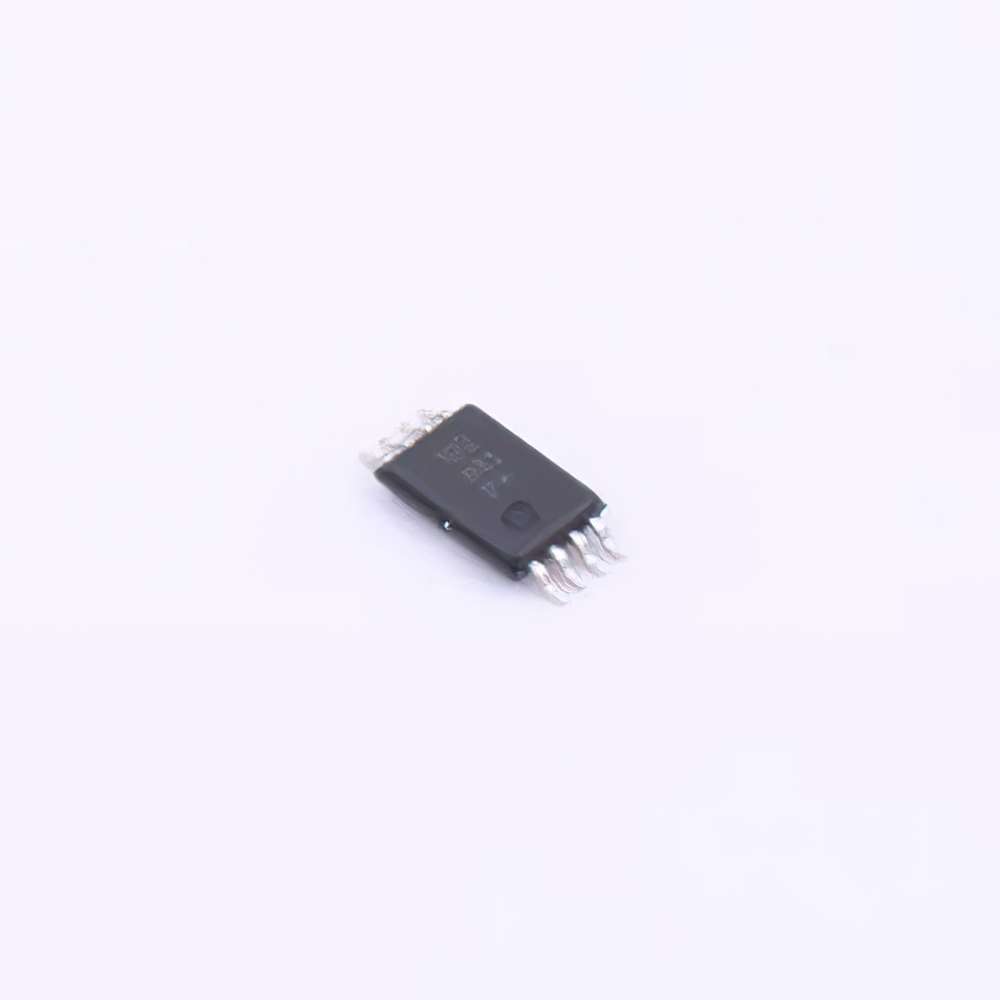
图片可能具有代表性。
产品详情请参阅规格.
产品详情请参阅规格.

NB3V8312CFAG
12 LVCMOS/LVTTL
型号
NB3V8312CFAG
类目
Logic Devices > Buffers/Drivers/Transceivers
制造商/品牌
onsemi (Ansemi)
封装
LQFP-32
包装
the tray
包裹数量
250
简介
The NB3V8312C is a high-performance, low-skew LVCMOS fan-out buffer that distributes 12 ultra-low-jitter clocks based on LVCMOS/LVTTL inputs up to 250 MHz. Twelve LVCMOS output pins drive 50Ω series or parallel terminated transmission lines. These outputs can also be disabled as high impedance (tri-state) via the OE input, or enabled when high. NB3V8312C provides an enable input, CLK_EN pin, which simultaneously enables the clock output, or disables it in a low state. Because this input is internally synchronized to the input clock and only changes when the input is low, there is no output glitch or runt pulse generation. Separate VDD core and VDDO output supplies allow the output buffer to operate at a supply voltage equal to VDD (VDD = VDDO) or lower. Dual-supply operation enables lower power consumption and output level compatibility compared to single-supply operation. The VDD core supply voltage can be set to 3.3 V, 2.5 V, or 1.8 V, and the VDDO output supply voltage can be set to 3.3 V, 2.5 V, or 1.8 V, but there is a constraint that VDD >/= VDDO.
请求报价
请填写所有必填字段并点击“提交”,我们将在12小时内通过电子邮件与您联系。如果您有任何问题,请留言或发送电子邮件至 2762329346@qq.com,我们将尽快回复。
有货 76988 PCS
联系信息
关键词 NB3V8312CFAG
NB3V8312CFAG 电子元件
NB3V8312CFAG 销售
NB3V8312CFAG 供应商
NB3V8312CFAG 分销商
NB3V8312CFAG 数据表
NB3V8312CFAG 图片
NB3V8312CFAG 报价
NB3V8312CFAG 提供
NB3V8312CFAG 最低价格
NB3V8312CFAG 搜索
NB3V8312CFAG 购买
NB3V8312CFAG 芯片
×
![]()

