onsemi (Ansemi)
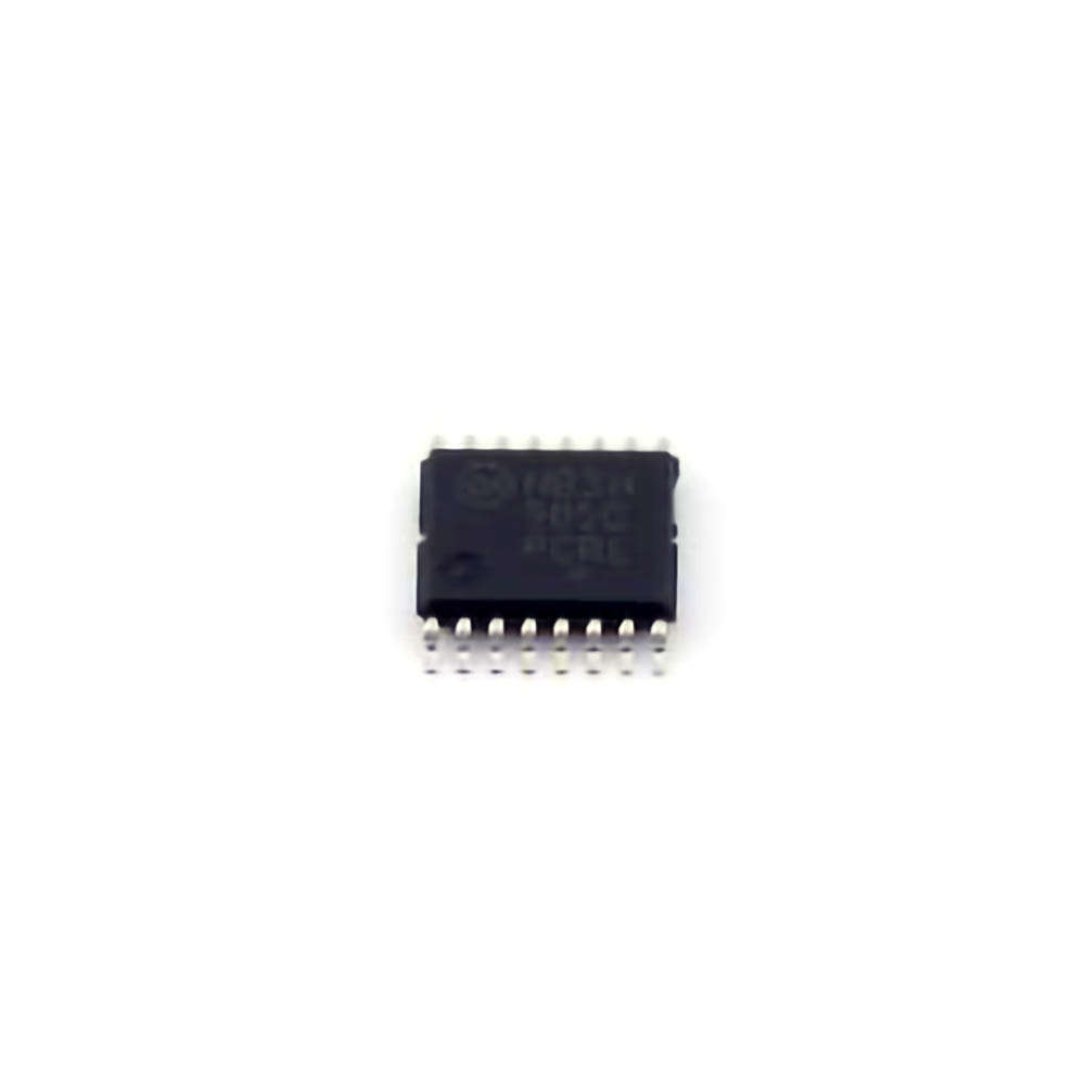
图片可能具有代表性。
产品详情请参阅规格.
产品详情请参阅规格.

NB3H5150MNTXG
Clock Generator, Multirate, Low Noise, 2.5V/3.3V
型号
NB3H5150MNTXG
类目
RTC/Clock Chip > Clock Generator/Frequency Synthesizer/PLL
制造商/品牌
onsemi (Ansemi)
封装
QFN-32-EP(5x5)
包装
taping
包裹数量
1000
简介
The NB3H5150 is a high-performance multi-rate clock growth stage that can simultaneously synthesize up to four different frequencies based on a single PLL using a 25 MHz input reference. The reference frequency can be a crystal, LVCMOS/LVTTL, LVPECL, HCSL or LVDS differential signal. The REFMODE pin selects the reference source. Three Output Groups (CLK1A/CLK1B to CLK3A/CLK3B) Generate User-Selectable Frequency: 25 MHz, 33.33 MHz, 50 MHz, 100 MHz, 125 MHz, or 156.25 MHz with Ultra-Low Noise/Jitter Performance < 0.3 ps . The fourth output bank (CLK4A/CLK4B) can generate the following integer and FRAC?N frequencies in pin-strap mode: 33.33 MHz, 66.66 MHz, 100 MHz, 106.25 MHz, 125 MHz, 133.33 MHz, 155.52 MHz, 156.25 MHz or 161.1328 MHz. More programmable frequencies are available through the I2C interface with less than 1 ps jitter performance. Detailed registration instructions will be provided in a future application note. Each output block can create two single-ended in-phase LVCMOS outputs or one LVPECL output differential pair. Each of the four output blocks can be individually powered from a separate VDDO, 2.5 V/3.3 V for LVPECL, 1.8 V/2.5 V/3.3 V for LVCMOS. The serial (I2C and SMBUS) interface is programmable for a variety of functions, including the frequency and output level of each divider block, and each block can be enabled and disabled individually.
请求报价
请填写所有必填字段并点击“提交”,我们将在12小时内通过电子邮件与您联系。如果您有任何问题,请留言或发送电子邮件至 2762329346@qq.com,我们将尽快回复。
有货 51179 PCS
联系信息
关键词 NB3H5150MNTXG
NB3H5150MNTXG 电子元件
NB3H5150MNTXG 销售
NB3H5150MNTXG 供应商
NB3H5150MNTXG 分销商
NB3H5150MNTXG 数据表
NB3H5150MNTXG 图片
NB3H5150MNTXG 报价
NB3H5150MNTXG 提供
NB3H5150MNTXG 最低价格
NB3H5150MNTXG 搜索
NB3H5150MNTXG 购买
NB3H5150MNTXG 芯片
×
![]()

