


AT45DB641E-SHN-T
IC FLASH 64MBIT 85MHZ 8SOIC
型号
AT45DB641E-SHN-T
制造商/品牌
系列
-
零件状态
Active
包装
Tape & Reel (TR)
技术
Flash
工作温度
-40°C ~ 85°C (TC)
安装类型
Surface Mount
封装/箱体
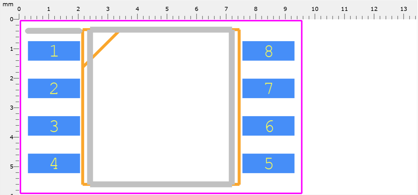
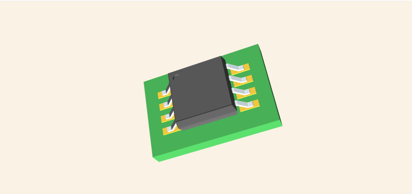
8-SOIC (0.209", 5.30mm Width)
供应商器件封装
8-SOIC
电压 - 电源
1.7 V ~ 3.6 V
内存类型
Non-Volatile
内存大小
64Mb (264 Bytes x 32K pages)
访问时间
-
时钟频率
85MHz
内存格式
Flash
写入周期时间 - 字、页
8µs, 5ms
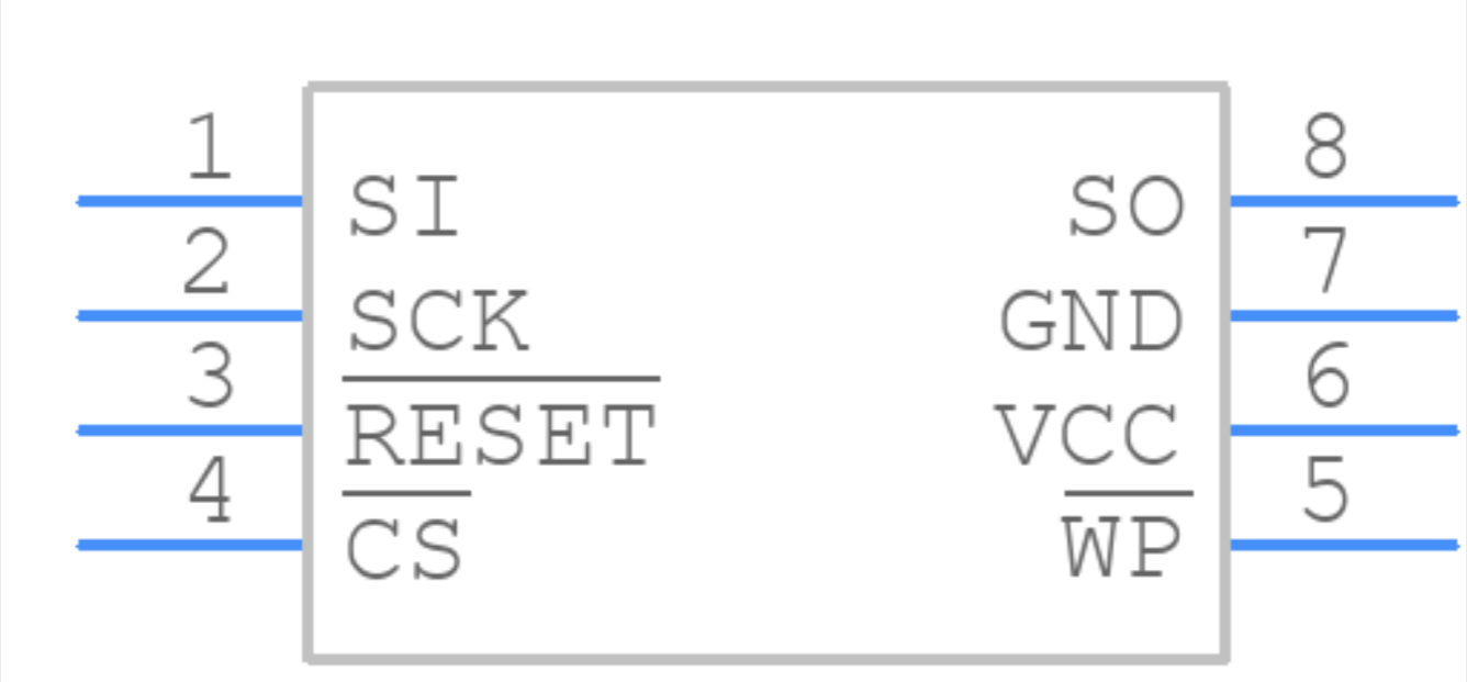
内存接口
SPI
请求报价
请填写所有必填字段并点击“提交”,我们将在12小时内通过电子邮件与您联系。如果您有任何问题,请留言或发送电子邮件至 2762329346@qq.com,我们将尽快回复。
有货 41652 PCS
联系信息
more_pkgimg
more_schimg
more_3dimg
more_desctext
The AT45DB641E DataFlash is a member of our System Enhancing class of code and data storage solutions designed with an advanced dual SRAM buffer architecture that makes it the most efficient memory for data logging. It also incorporates a suite of advanced features that save system power, reduce processor overhead, simplify software development, and provide comprehensive data security and integrity options.
Pin Count--------8
Part Category--------Integrated Circuit
Package Category--------Small Outline Packages
Footprint Name--------Small Outline Packages - 8S2 - 8-lead, 0.208''Wide EIAJ SOIC
Pin Count--------8
Part Category--------Integrated Circuit
Package Category--------Small Outline Packages
Footprint Name--------Small Outline Packages - 8S2 - 8-lead, 0.208''Wide EIAJ SOIC
download_pdf
more_faq
AT45DB641E-SHN-T Frequently Asked Questions (FAQs)
What is the recommended operating voltage range for the AT45DB641E-SHN-T?
The recommended operating voltage range for the AT45DB641E-SHN-T is 2.7V to 3.6V.
How do I handle the HOLD pin during power-up and power-down sequences?
The HOLD pin should be pulled high during power-up and power-down sequences to prevent unwanted data corruption.
What is the maximum number of erase cycles supported by the AT45DB641E-SHN-T?
The AT45DB641E-SHN-T supports up to 100,000 erase cycles.
How do I implement wear leveling to extend the lifespan of the device?
Wear leveling can be implemented by distributing erase cycles across the entire memory space, using techniques such as dynamic wear leveling or static wear leveling.
What is the purpose of the WP (Write Protect) pin?
The WP pin is used to prevent accidental writes to the device. When the WP pin is low, the device is in a write-protected state.
相关产品

关键词 AT45DB641E-SHN-T
AT45DB641E-SHN-T 电子元件
AT45DB641E-SHN-T 销售
AT45DB641E-SHN-T 供应商
AT45DB641E-SHN-T 分销商
AT45DB641E-SHN-T 数据表
AT45DB641E-SHN-T 图片
AT45DB641E-SHN-T 报价
AT45DB641E-SHN-T 提供
AT45DB641E-SHN-T 最低价格
AT45DB641E-SHN-T 搜索
AT45DB641E-SHN-T 购买
AT45DB641E-SHN-T 芯片
×
![]()