
ADI (Adeno)
图片可能具有代表性。
产品详情请参阅规格.
产品详情请参阅规格.
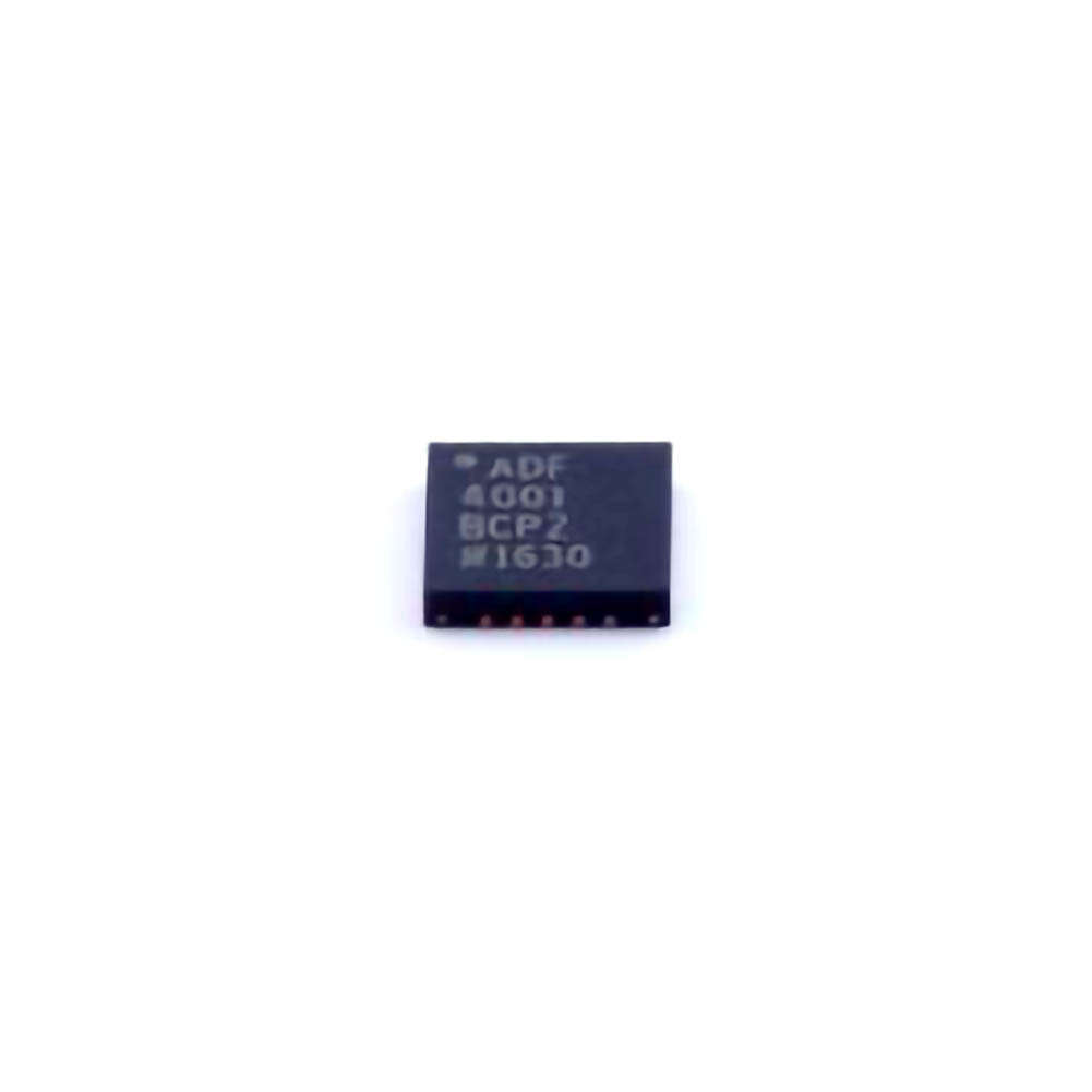
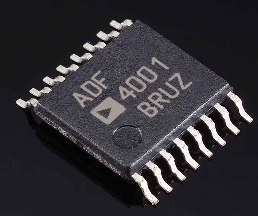
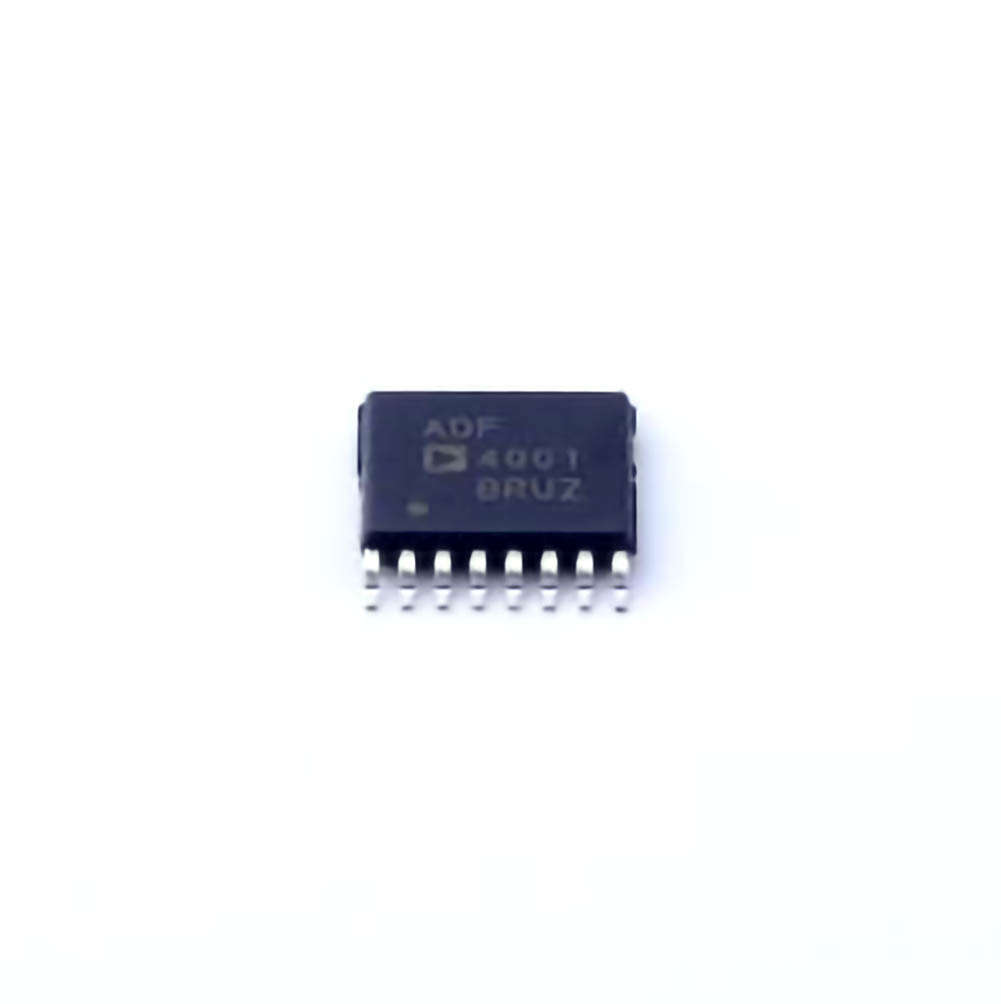
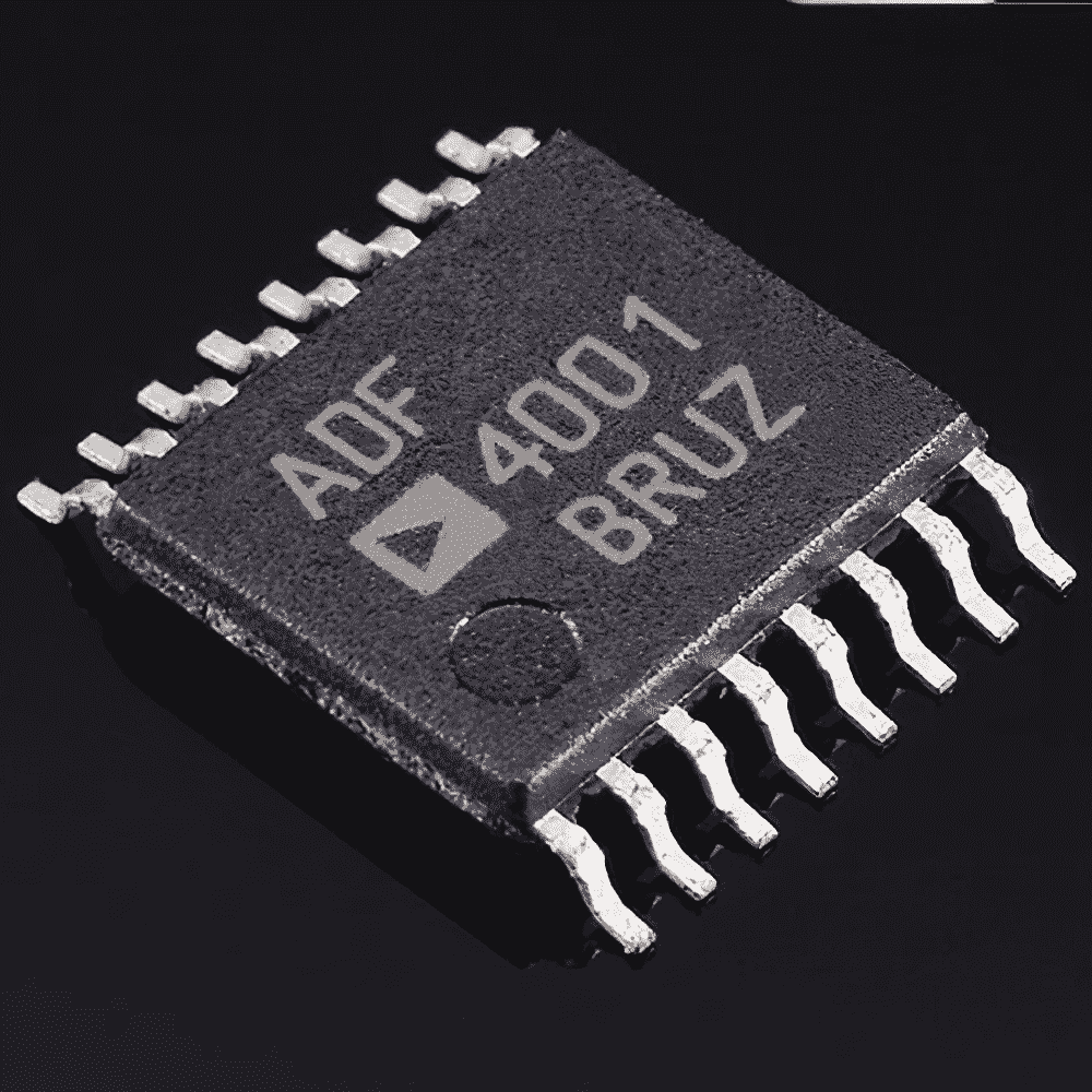
ADF4350BCPZ-RL7
ADF4350BCPZ-RL7
型号
ADF4350BCPZ-RL7
类目
RTC/Clock Chip > Clock Generator/Frequency Synthesizer/PLL
制造商/品牌
ADI (Adeno)
封装
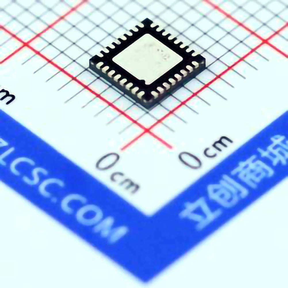
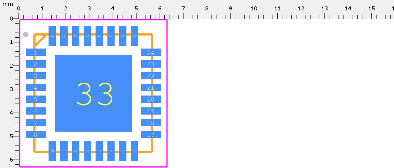
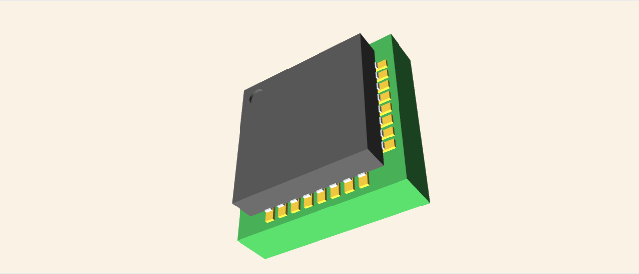
LFCSP-32
包装
taping
包裹数量
1500
简介
请求报价
请填写所有必填字段并点击“提交”,我们将在12小时内通过电子邮件与您联系。如果您有任何问题,请留言或发送电子邮件至 2762329346@qq.com,我们将尽快回复。
有货 50591 PCS
联系信息
more_pkgimg
more_schimg
more_3dimg
more_spec
ADF4350BCPZ Product details
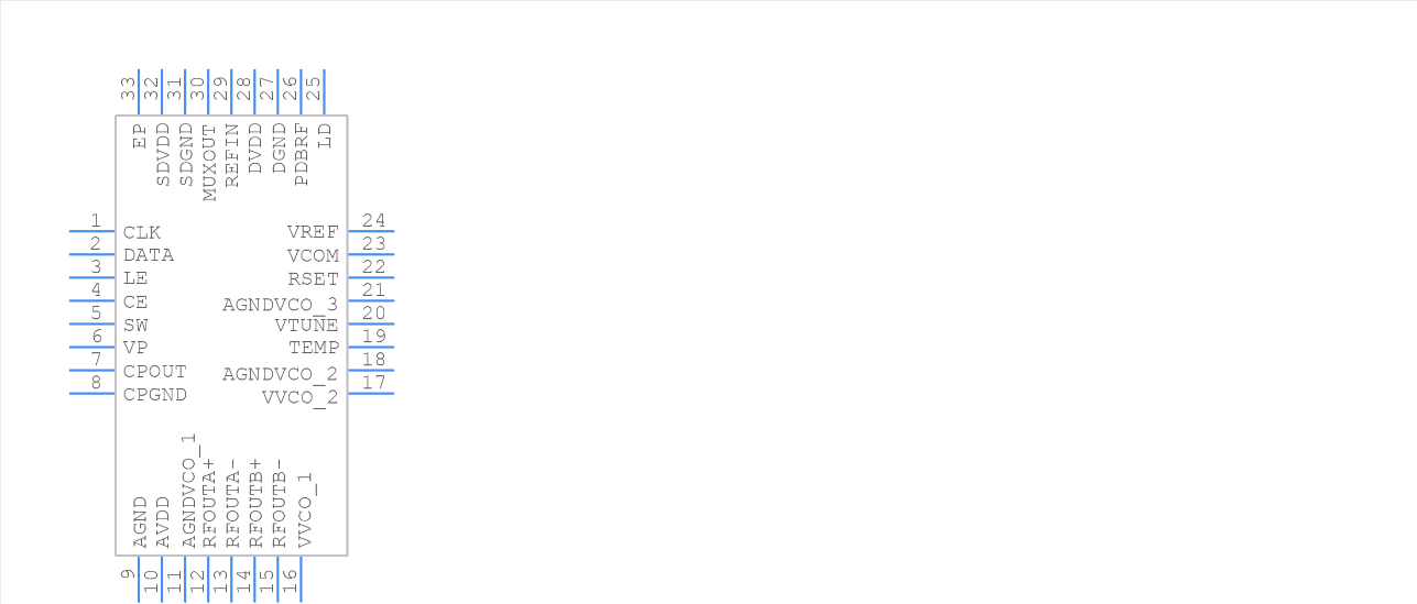
The ADF4350 allows implementation of fractional-N or integer-N phase-locked loop (PLL) frequency synthesizers if used with an external loop filter and external reference frequency.
The ADF4350 has an integrated voltage controlled oscillator (VCO) with a fundamental output frequency ranging from 2200 MHz to 4400 MHz.
more_desctext
137.5-4400MHz Synthesizer with VCO LFCSP Analog Devices ADF4350BCPZ, Dual PLL Clock Synthesizer, 137.5 → 4400 MHz, 32-Pin LFCSP VQ
Pin Count--------33
Part Category--------Integrated Circuit
Package Category--------Quad Flat No-Lead
Footprint Name--------Quad Flat No-Lead - CP-32-2(LFCSP_VQ)
Pin Count--------33
Part Category--------Integrated Circuit
Package Category--------Quad Flat No-Lead
Footprint Name--------Quad Flat No-Lead - CP-32-2(LFCSP_VQ)
download_pdf
more_faq
ADF4350BCPZ Frequently Asked Questions (FAQs)
What is the recommended power-up sequence for the ADF4350?
The recommended power-up sequence is to apply VDD first, followed by AVDD, and then DVDD. This ensures that the internal voltage regulators are powered up correctly.
How do I optimize the loop filter design for the ADF4350?
The loop filter design depends on the specific application and requirements. A good starting point is to use the recommended values in the datasheet, and then optimize the filter components based on the desired phase noise and spurious performance.
What is the maximum frequency deviation that can be achieved with the ADF4350?
The maximum frequency deviation is dependent on the charge pump current and the loop bandwidth. The datasheet provides a formula to calculate the maximum frequency deviation, which is approximately 10 MHz for a charge pump current of 2.5 mA and a loop bandwidth of 100 kHz.
How do I troubleshoot PLL lock issues with the ADF4350?
To troubleshoot PLL lock issues, check the power supply voltages, ensure that the reference clock is stable, and verify that the loop filter components are correct. Also, check the lock detect output (LD) to ensure that the PLL is locking correctly.
What is the recommended PCB layout and thermal management for the ADF4350?
A good PCB layout practice is to keep the analog and digital grounds separate, and to use a solid ground plane to reduce noise. For thermal management, ensure good airflow around the device, and consider using a heat sink if the device is expected to operate at high temperatures.
相关产品

关键词 ADF4350BCPZ-RL7
ADF4350BCPZ-RL7 电子元件
ADF4350BCPZ-RL7 销售
ADF4350BCPZ-RL7 供应商
ADF4350BCPZ-RL7 分销商
ADF4350BCPZ-RL7 数据表
ADF4350BCPZ-RL7 图片
ADF4350BCPZ-RL7 报价
ADF4350BCPZ-RL7 提供
ADF4350BCPZ-RL7 最低价格
ADF4350BCPZ-RL7 搜索
ADF4350BCPZ-RL7 购买
ADF4350BCPZ-RL7 芯片
×
![]()