

NSBC113EPDXV6T1G
Product Overview
- Category: Semiconductor/Electronic Component
- Use: Power Transistor
- Characteristics: High power handling, low on-resistance, fast switching speed
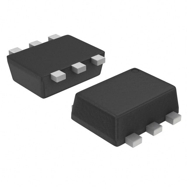
- Package: TO-252-3 (DPAK)
- Essence: Efficient power management
- Packaging/Quantity: Tape & Reel, 2500 units per reel
Specifications
- Voltage Rating: 60V
- Current Rating: 10A
- On-Resistance: 25mΩ
- Power Dissipation: 2.5W
- Operating Temperature Range: -55°C to 150°C
Detailed Pin Configuration
The NSBC113EPDXV6T1G has a standard TO-252-3 pin configuration with the following pinout: 1. Pin 1: Source 2. Pin 2: Gate 3. Pin 3: Drain
Functional Features
- Fast switching speed for efficient power management
- Low on-resistance for minimal power loss
- High power handling capability for robust performance
Advantages and Disadvantages
Advantages
- Efficient power management
- Fast switching speed
- Low on-resistance
Disadvantages
- Limited voltage and current ratings compared to higher-end models
- Sensitive to overvoltage conditions
Working Principles
The NSBC113EPDXV6T1G operates based on the principles of field-effect transistors, utilizing the control of electric fields to modulate the flow of current between the source and drain terminals.
Detailed Application Field Plans
The NSBC113EPDXV6T1G is suitable for various applications including: - Switching power supplies - Motor control - LED lighting - Battery management systems
Detailed and Complete Alternative Models
- Alternative Model 1: NSBC114EPDXV6T1G
- Similar specifications and package type
- Alternative Model 2: NSBC115EPDXV6T1G
- Higher voltage and current ratings, same package type
This comprehensive entry provides a detailed overview of the NSBC113EPDXV6T1G, covering its basic information, specifications, pin configuration, functional features, advantages and disadvantages, working principles, application field plans, and alternative models, offering valuable insights for users and engineers in the semiconductor industry.
10个与NSBC113EPDXV6T1G在技术解决方案中的应用相关的常见问题及解答
What is NSBC113EPDXV6T1G?
- NSBC113EPDXV6T1G is a high-performance NPN bipolar junction transistor (BJT) designed for use in various technical solutions.
What are the key features of NSBC113EPDXV6T1G?
- The key features include high current capability, low saturation voltage, and fast switching speed, making it suitable for power management and other technical applications.
In what technical solutions can NSBC113EPDXV6T1G be used?
- NSBC113EPDXV6T1G can be used in applications such as voltage regulators, DC-DC converters, motor control, and electronic lighting systems.
What is the maximum operating temperature for NSBC113EPDXV6T1G?
- The maximum operating temperature for NSBC113EPDXV6T1G is typically around 150°C, making it suitable for a wide range of operating conditions.
What is the typical gain of NSBC113EPDXV6T1G?
- The typical gain of NSBC113EPDXV6T1G is in the range of 100 to 300, ensuring reliable amplification in various technical solutions.
Does NSBC113EPDXV6T1G require any external components for operation?
- NSBC113EPDXV6T1G may require external resistors or capacitors depending on the specific application, but it is designed for straightforward integration into technical solutions.
What are the recommended storage conditions for NSBC113EPDXV6T1G?
- It is recommended to store NSBC113EPDXV6T1G in a dry environment with a temperature range between -55°C to 150°C to maintain its performance and reliability.
Can NSBC113EPDXV6T1G be used in automotive applications?
- Yes, NSBC113EPDXV6T1G is suitable for automotive applications due to its robust design and ability to withstand harsh environmental conditions.
What are the typical input and output capacitances of NSBC113EPDXV6T1G?
- The typical input and output capacitances of NSBC113EPDXV6T1G are in the range of a few picofarads, minimizing the impact on high-frequency performance in technical solutions.
Is NSBC113EPDXV6T1G RoHS compliant?
- Yes, NSBC113EPDXV6T1G is RoHS compliant, meeting environmental standards for lead-free and hazardous substance-free materials.