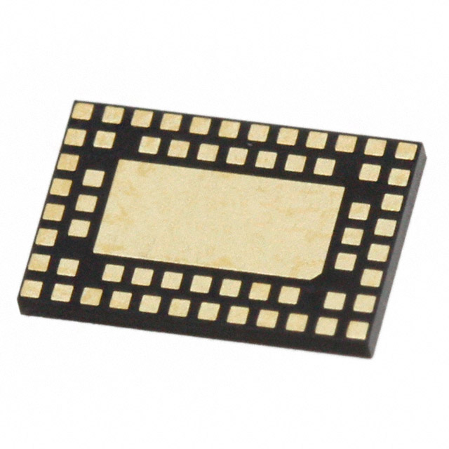
74LVC16374ABX,518
Basic Information Overview
- Category: Integrated Circuit (IC)
- Use: Flip-Flop
- Characteristics: Low-voltage CMOS, 16-bit D-type flip-flop with 3-state outputs
- Package: TSSOP (Thin Shrink Small Outline Package)
- Essence: Sequential logic device for storing and transferring binary data
- Packaging/Quantity: Tape and Reel, 2500 units per reel
Specifications
- Supply Voltage Range: 1.65V to 5.5V
- High-Level Input Voltage: 2V to VCC + 0.5V
- Low-Level Input Voltage: -0.5V to 0.8V
- High-Level Output Voltage: 2.4V (min) at IOH = -24mA
- Low-Level Output Voltage: 0.4V (max) at IOL = 24mA
- Operating Temperature Range: -40°C to +125°C
Detailed Pin Configuration
The 74LVC16374ABX,518 IC has a total of 48 pins. The pin configuration is as follows:
- Pin 1: Data Input (D0)
- Pin 2: Data Input (D1)
- Pin 3: Data Input (D2)
- Pin 4: Data Input (D3)
- Pin 5: Data Input (D4)
- Pin 6: Data Input (D5)
- Pin 7: Data Input (D6)
- Pin 8: Data Input (D7)
- Pin 9: Data Input (D8)
- Pin 10: Data Input (D9)
- Pin 11: Data Input (D10)
- Pin 12: Data Input (D11)
- Pin 13: Data Input (D12)
- Pin 14: Data Input (D13)
- Pin 15: Data Input (D14)
- Pin 16: Data Input (D15)
- Pin 17: Clock Input (CP)
- Pin 18: Clock Enable Input (CE)
- Pin 19: Output Enable Input (OE)
- Pin 20: Master Reset Input (MR)
- Pin 21: Data Output (Q0)
- Pin 22: Data Output (Q1)
- Pin 23: Data Output (Q2)
- Pin 24: Data Output (Q3)
- Pin 25: Data Output (Q4)
- Pin 26: Data Output (Q5)
- Pin 27: Data Output (Q6)
- Pin 28: Data Output (Q7)
- Pin 29: Data Output (Q8)
- Pin 30: Data Output (Q9)
- Pin 31: Data Output (Q10)
- Pin 32: Data Output (Q11)
- Pin 33: Data Output (Q12)
- Pin 34: Data Output (Q13)
- Pin 35: Data Output (Q14)
- Pin 36: Data Output (Q15)
- Pin 37: GND (Ground)
- Pin 38: GND (Ground)
- Pin 39: GND (Ground)
- Pin 40: VCC (Supply Voltage)
Functional Features
- 16-bit D-type flip-flop with 3-state outputs
- Non-inverting data path for easy cascading
- High-speed operation, suitable for various applications
- 3-state outputs allow multiple devices to share a common bus
- Low power consumption and wide supply voltage range
Advantages and Disadvantages
Advantages: - High-speed operation enables efficient data transfer - Non-inverting data path simplifies cascading of multiple flip-flops - 3-state outputs facilitate bus sharing among multiple devices - Wide supply voltage range allows compatibility with different systems
Disadvantages: - Limited number of flip-flops (16-bit) in a single IC package - TSSOP package may require careful handling during assembly
Working Principles
The 74LVC16374ABX,518 is a 16-bit D-type flip-flop that stores and transfers binary data. It operates based on clock signals and can be enabled or disabled using control inputs. The non-inverting data path ensures that the stored data is transferred without any inversion. The 3-state outputs allow the device to be connected to a common bus, enabling multiple devices to share the same data lines.
Detailed Application Field Plans
The 74LVC16374ABX,518 IC finds applications in various fields, including: 1. Microprocessor-based systems
10个与74LVC16374ABX,518在技术解决方案中的应用相关的常见问题及解答
Sure! Here are 10 common questions and answers related to the application of 74LVC16374ABX,518 in technical solutions:
Q: What is the function of the 74LVC16374ABX,518? A: The 74LVC16374ABX,518 is a 16-bit D-type flip-flop with 3-state outputs. It can store and transfer data in digital circuits.
Q: What is the operating voltage range for the 74LVC16374ABX,518? A: The 74LVC16374ABX,518 operates within a voltage range of 1.65V to 5.5V.
Q: How many flip-flops are there in the 74LVC16374ABX,518? A: The 74LVC16374ABX,518 contains 16 individual D-type flip-flops.
Q: Can the 74LVC16374ABX,518 be used for bidirectional data transfer? A: Yes, the 74LVC16374ABX,518 supports bidirectional data flow, making it suitable for applications requiring data transfer in both directions.
Q: What is the maximum clock frequency supported by the 74LVC16374ABX,518? A: The 74LVC16374ABX,518 can operate at a maximum clock frequency of 125 MHz.
Q: Does the 74LVC16374ABX,518 have internal pull-up or pull-down resistors? A: No, the 74LVC16374ABX,518 does not have internal pull-up or pull-down resistors. External resistors may be required if needed.
Q: Can the 74LVC16374ABX,518 be used in high-speed applications? A: Yes, the 74LVC16374ABX,518 is designed for high-speed operation and can be used in various high-frequency applications.
Q: What is the output drive capability of the 74LVC16374ABX,518? A: The 74LVC16374ABX,518 has a balanced output drive with both sourcing and sinking capabilities.
Q: Is the 74LVC16374ABX,518 compatible with other logic families? A: Yes, the 74LVC16374ABX,518 is compatible with both TTL and CMOS logic families, making it versatile for integration into different systems.
Q: Can the 74LVC16374ABX,518 be cascaded to increase the number of flip-flops? A: Yes, multiple 74LVC16374ABX,518 ICs can be cascaded together to increase the number of flip-flops and expand the storage capacity in a circuit.
Please note that the specific part number mentioned (74LVC16374ABX,518) may vary depending on the manufacturer or distributor.


