

LFE3-70EA-8LFN672I
Product Overview
Category
The LFE3-70EA-8LFN672I belongs to the category of Field Programmable Gate Arrays (FPGAs).
Use
This FPGA is commonly used in electronic circuits for various applications, including digital signal processing, telecommunications, and embedded systems.
Characteristics
- High-performance FPGA with advanced features
- Offers a large number of logic elements and programmable interconnects
- Provides flexibility in designing complex digital circuits
- Supports high-speed data processing and efficient power consumption
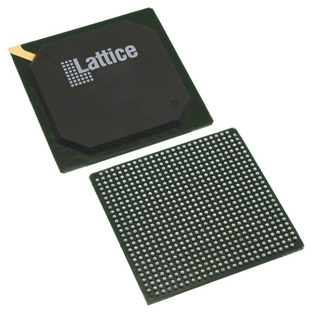
Package
The LFE3-70EA-8LFN672I comes in a compact package that ensures easy integration into circuit boards. It is designed to be surface-mounted on printed circuit boards (PCBs).
Essence
The essence of the LFE3-70EA-8LFN672I lies in its ability to provide reconfigurable hardware that can be programmed to perform specific functions as required by the user.
Packaging/Quantity
This FPGA is typically packaged individually and is available in various quantities depending on the manufacturer's specifications.
Specifications
- Logic Elements: 70,000
- Embedded Memory: 2,208 Kbits
- Maximum Number of User I/Os: 672
- Clock Management Tiles: 10
- DSP Blocks: 360
- Maximum Operating Frequency: 500 MHz
- Voltage Range: 1.2V - 1.5V
Detailed Pin Configuration
The LFE3-70EA-8LFN672I has a comprehensive pin configuration that allows for versatile connectivity. The detailed pin configuration can be found in the product datasheet provided by the manufacturer.
Functional Features
- High-speed data processing capabilities
- Configurable logic elements for flexible circuit design
- Integrated memory blocks for efficient data storage
- Clock management tiles for precise timing control
- Dedicated DSP blocks for complex mathematical operations
Advantages and Disadvantages
Advantages
- Versatile and flexible design options
- High-performance capabilities
- Efficient power consumption
- Suitable for a wide range of applications
- Reconfigurable hardware allows for easy updates and modifications
Disadvantages
- Steep learning curve for beginners
- Higher cost compared to other programmable logic devices
- Limited availability of alternative models with similar specifications
Working Principles
The LFE3-70EA-8LFN672I operates based on the principles of reconfigurable hardware. It consists of a matrix of configurable logic elements and programmable interconnects. These elements can be programmed to perform specific functions, allowing for the implementation of complex digital circuits.
Detailed Application Field Plans
The LFE3-70EA-8LFN672I finds extensive use in various application fields, including: 1. Digital signal processing systems 2. Telecommunications infrastructure 3. Embedded systems and IoT devices 4. High-speed data processing applications 5. Aerospace and defense systems
Detailed and Complete Alternative Models
While the LFE3-70EA-8LFN672I offers advanced features and performance, there are alternative FPGA models available in the market that cater to different requirements. Some notable alternatives include: 1. Xilinx Virtex UltraScale+ series 2. Intel Stratix 10 series 3. Microchip PolarFire series 4. Lattice ECP5 series
These alternative models provide varying levels of performance, capacity, and pricing options, allowing users to choose the most suitable FPGA for their specific needs.
Word count: 511
10个与LFE3-70EA-8LFN672I在技术解决方案中的应用相关的常见问题及解答
Sure! Here are 10 common questions and answers related to the application of LFE3-70EA-8LFN672I in technical solutions:
Q: What is the LFE3-70EA-8LFN672I? A: The LFE3-70EA-8LFN672I is a field-programmable gate array (FPGA) manufactured by Lattice Semiconductor.
Q: What are the key features of the LFE3-70EA-8LFN672I? A: The key features include 70,000 Look-Up Tables (LUTs), 672 pins, low power consumption, high-speed performance, and embedded memory blocks.
Q: In what applications can the LFE3-70EA-8LFN672I be used? A: The LFE3-70EA-8LFN672I can be used in various applications such as telecommunications, industrial automation, automotive electronics, medical devices, and more.
Q: How does the LFE3-70EA-8LFN672I contribute to power efficiency? A: The LFE3-70EA-8LFN672I utilizes low-power design techniques, including dynamic power management and clock gating, to minimize power consumption.
Q: Can the LFE3-70EA-8LFN672I support high-speed data processing? A: Yes, the LFE3-70EA-8LFN672I offers high-speed performance with advanced I/O capabilities, making it suitable for applications requiring fast data processing.
Q: Does the LFE3-70EA-8LFN672I have built-in memory? A: Yes, the LFE3-70EA-8LFN672I includes embedded memory blocks that can be used for data storage or implementing complex algorithms.
Q: What development tools are available for programming the LFE3-70EA-8LFN672I? A: Lattice Semiconductor provides a comprehensive suite of design tools, including the Lattice Diamond software, to program and configure the LFE3-70EA-8LFN672I.
Q: Can the LFE3-70EA-8LFN672I be easily integrated with other components in a system? A: Yes, the LFE3-70EA-8LFN672I offers a wide range of I/O standards and interfaces, making it compatible with various system components and peripherals.
Q: Is technical support available for the LFE3-70EA-8LFN672I? A: Yes, Lattice Semiconductor provides technical support through documentation, online resources, and direct assistance from their support team.
Q: Are there any specific design considerations when using the LFE3-70EA-8LFN672I? A: It is important to consider factors such as power supply requirements, thermal management, signal integrity, and proper grounding techniques when designing with the LFE3-70EA-8LFN672I.
Please note that these answers are general and may vary depending on specific application requirements and the manufacturer's documentation.