

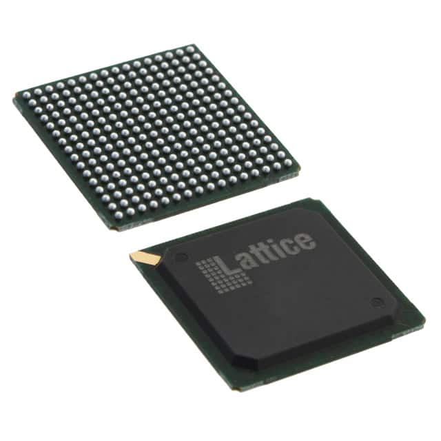
LFE2M35SE-5FN256I
Product Overview
Category
The LFE2M35SE-5FN256I belongs to the category of Field Programmable Gate Arrays (FPGAs).
Use
This FPGA is primarily used for digital logic design and implementation in various electronic systems.
Characteristics
- High-performance programmable logic device
- Offers flexibility and reconfigurability
- Provides a large number of configurable logic blocks (CLBs)
- Supports complex digital circuit designs
- Enables rapid prototyping and development
Package
The LFE2M35SE-5FN256I comes in a 256-pin FineLine BGA package.
Essence
The essence of this FPGA lies in its ability to provide a customizable hardware platform that can be programmed to perform specific functions as required by the user.
Packaging/Quantity
The LFE2M35SE-5FN256I is typically packaged individually and is available in various quantities depending on the customer's requirements.
Specifications
- Device Family: LatticeECP2M
- Logic Elements: 33,216
- Embedded Memory: 1,152 Kbits
- Maximum User I/Os: 202
- Operating Voltage: 1.2V
- Speed Grade: -5
- Package Type: FineLine BGA
- Package Pins: 256
- Temperature Range: Commercial (0°C to 85°C)
Detailed Pin Configuration
For a detailed pin configuration diagram of the LFE2M35SE-5FN256I, please refer to the manufacturer's datasheet or technical documentation.
Functional Features
- High-speed performance with low power consumption
- Configurable I/O standards and voltage levels
- Built-in memory blocks for efficient data storage
- Dedicated clock management resources
- Support for various communication protocols
- On-chip PLLs for clock generation and synchronization
Advantages and Disadvantages
Advantages
- Flexibility to implement custom logic designs
- Faster time-to-market for electronic systems
- Reconfigurability allows for design iterations and updates
- Lower development costs compared to ASICs
- Suitable for prototyping and low-volume production
Disadvantages
- Higher power consumption compared to dedicated hardware solutions
- Limited performance compared to application-specific devices
- Steeper learning curve for FPGA programming and design
Working Principles
The LFE2M35SE-5FN256I operates based on the principles of reconfigurable computing. It consists of a matrix of configurable logic blocks (CLBs) interconnected through programmable routing resources. The user can program the FPGA using a Hardware Description Language (HDL) to define the desired digital circuit functionality. Upon configuration, the FPGA executes the programmed logic, enabling the implementation of complex digital systems.
Detailed Application Field Plans
The LFE2M35SE-5FN256I finds applications in various fields, including:
- Telecommunications: Used in base stations, network switches, and routers for signal processing and protocol handling.
- Industrial Automation: Employed in control systems, motor drives, and robotics for real-time data processing and control algorithms.
- Automotive Electronics: Utilized in automotive control units, infotainment systems, and driver assistance systems for advanced functionalities.
- Aerospace and Defense: Integrated into avionics systems, radar systems, and communication equipment for high-performance signal processing and encryption.
- Consumer Electronics: Incorporated in smart TVs, gaming consoles, and wearable devices for multimedia processing and user interface control.
Detailed and Complete Alternative Models
- Xilinx Virtex-7 XC7VX485T FPGA
- Intel Cyclone V EP5CE115F23I7N FPGA
- Microsemi SmartFusion2 M2S010S FPGA
- Actel ProASIC3 A3P1000 FPGA
- QuickLogic PolarPro 3E FPGA
These alternative models offer similar capabilities and can be considered as alternatives to the LFE2M35SE-5FN256I based on specific project requirements.
Note: The content provided above is a sample entry and may not reflect actual specifications or details of the mentioned product.
10个与LFE2M35SE-5FN256I在技术解决方案中的应用相关的常见问题及解答
Sure! Here are 10 common questions and answers related to the application of LFE2M35SE-5FN256I in technical solutions:
Q: What is the LFE2M35SE-5FN256I? A: The LFE2M35SE-5FN256I is a specific model of Field-Programmable Gate Array (FPGA) manufactured by Lattice Semiconductor.
Q: What are the key features of the LFE2M35SE-5FN256I? A: Some key features of this FPGA include 35,000 Look-Up Tables (LUTs), 256-pin FineLine BGA package, 5V tolerant I/Os, and support for various communication protocols.
Q: What are the typical applications of the LFE2M35SE-5FN256I? A: This FPGA is commonly used in applications such as industrial automation, automotive electronics, telecommunications, medical devices, and consumer electronics.
Q: How can I program the LFE2M35SE-5FN256I? A: The LFE2M35SE-5FN256I can be programmed using Lattice Diamond design software or other compatible programming tools provided by Lattice Semiconductor.
Q: Can I use the LFE2M35SE-5FN256I for high-speed data processing? A: Yes, the LFE2M35SE-5FN256I supports high-speed data processing with its advanced architecture and optimized routing resources.
Q: Does the LFE2M35SE-5FN256I support different communication interfaces? A: Yes, this FPGA supports various communication interfaces such as UART, SPI, I2C, Ethernet, PCIe, and USB, making it versatile for different applications.
Q: Can I use the LFE2M35SE-5FN256I for real-time signal processing? A: Absolutely, the LFE2M35SE-5FN256I is capable of real-time signal processing due to its high-performance capabilities and low-latency architecture.
Q: What are the power requirements for the LFE2M35SE-5FN256I? A: The LFE2M35SE-5FN256I operates at a typical voltage range of 1.14V to 1.26V, with a maximum power consumption of around 1.5W.
Q: Is the LFE2M35SE-5FN256I suitable for low-power applications? A: Yes, this FPGA offers power-saving features such as dynamic power management and clock gating, making it suitable for low-power applications.
Q: Where can I find additional technical documentation and support for the LFE2M35SE-5FN256I? A: You can find detailed technical documentation, datasheets, application notes, and support resources on the official website of Lattice Semiconductor or by contacting their customer support team.
Please note that the answers provided here are general and may vary depending on specific design requirements and application scenarios.