

LFE2-35E-6FN484I
Product Overview
Category
The LFE2-35E-6FN484I belongs to the category of Field Programmable Gate Arrays (FPGAs).
Use
This FPGA is commonly used in electronic circuits for various applications such as digital signal processing, data communication, and embedded systems.
Characteristics
- High flexibility: The LFE2-35E-6FN484I offers a high level of programmability, allowing users to configure the device according to their specific requirements.
- High performance: With its advanced architecture and optimized design, this FPGA delivers excellent performance in terms of speed and efficiency.
- Low power consumption: The LFE2-35E-6FN484I is designed to minimize power consumption, making it suitable for battery-powered devices or energy-efficient applications.
- Large capacity: This FPGA provides a generous amount of logic elements and memory blocks, enabling the implementation of complex designs.
Package and Quantity
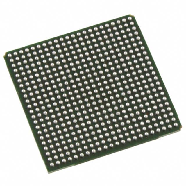
The LFE2-35E-6FN484I comes in a 484-pin FineLine BGA package. Each package contains one unit of the FPGA.
Specifications
- Logic Elements: 35,000
- Embedded Memory: 1,080 Kbits
- Maximum User I/Os: 316
- Clock Management Tiles: 4
- DSP Blocks: 40
- Operating Voltage: 1.2V
- Operating Temperature Range: -40°C to 100°C
Detailed Pin Configuration
For a detailed pin configuration diagram of the LFE2-35E-6FN484I, please refer to the manufacturer's datasheet or documentation.
Functional Features
- Configurable Logic Blocks (CLBs): The FPGA consists of multiple CLBs that can be programmed to perform various logical functions.
- Dedicated Routing Resources: The device provides dedicated routing resources to efficiently connect different components within the FPGA.
- Clock Management: The LFE2-35E-6FN484I includes clock management tiles that enable precise control and distribution of clock signals.
- Embedded Memory: This FPGA incorporates embedded memory blocks, allowing for efficient storage and retrieval of data.
- DSP Blocks: The device features dedicated Digital Signal Processing (DSP) blocks, which are optimized for performing complex mathematical operations.
Advantages and Disadvantages
Advantages
- High flexibility and programmability
- Excellent performance and speed
- Low power consumption
- Ample logic elements and memory capacity
Disadvantages
- Relatively high cost compared to other programmable logic devices
- Steeper learning curve for programming and design implementation
Working Principles
The LFE2-35E-6FN484I operates based on the principles of reconfigurable computing. It consists of a matrix of configurable logic blocks interconnected through programmable routing resources. Users can program the FPGA using Hardware Description Languages (HDLs) to define the desired functionality and interconnections of the logic elements.
Once programmed, the FPGA executes the specified logic functions by routing signals through the configured paths. The embedded memory and DSP blocks enhance the device's capabilities, enabling it to perform complex computations and store intermediate results.
Detailed Application Field Plans
The LFE2-35E-6FN484I finds applications in various fields, including:
- Communications: Used in networking equipment, routers, and switches for data packet processing and protocol handling.
- Industrial Automation: Employed in control systems, motor drives, and robotics for real-time control and signal processing.
- Aerospace and Defense: Utilized in radar systems, avionics, and military communication equipment for high-performance signal processing and encryption.
- Medical Devices: Integrated into medical imaging systems, patient monitoring devices, and diagnostic equipment for data processing and analysis.
- Automotive: Applied in advanced driver assistance systems (ADAS), engine control units (ECUs), and infotainment systems for efficient data processing and control.
Detailed and Complete Alternative Models
- LFE2-35E-5FN484I: Similar to the LFE2-35E-6FN484I, but with a lower logic element count.
- LFE2-35E-7FN484I: Similar to the LFE2-35E-6FN484I, but with a higher logic element count.
- LFE2-35E-6F672I: A variant with a different package and increased embedded memory capacity.
These alternative models offer similar functionality and can be considered based on specific project requirements.
In conclusion, the LFE2-35E-6FN484I is a versatile FPGA that combines high flexibility, performance, and low power consumption. Its extensive range of applications, along with various alternative models, make it a popular choice among designers and engineers in the field of digital electronics.
Word Count: 570
10个与LFE2-35E-6FN484I在技术解决方案中的应用相关的常见问题及解答
Sure! Here are 10 common questions and answers related to the application of LFE2-35E-6FN484I in technical solutions:
Q: What is the LFE2-35E-6FN484I? A: The LFE2-35E-6FN484I is a specific model of Field-Programmable Gate Array (FPGA) manufactured by Lattice Semiconductor.
Q: What are the key features of the LFE2-35E-6FN484I? A: The key features include 35,000 Look-Up Tables (LUTs), 6-input function capability, 484-pin FineLine BGA package, and low power consumption.
Q: What are some typical applications for the LFE2-35E-6FN484I? A: The LFE2-35E-6FN484I is commonly used in various technical solutions such as industrial automation, telecommunications, automotive electronics, medical devices, and consumer electronics.
Q: How can I program the LFE2-35E-6FN484I? A: The LFE2-35E-6FN484I can be programmed using hardware description languages (HDL) like VHDL or Verilog, which are then synthesized and implemented using appropriate software tools provided by Lattice Semiconductor.
Q: What are the advantages of using the LFE2-35E-6FN484I in technical solutions? A: Some advantages include its flexibility, reprogrammability, high performance, low power consumption, and ability to integrate multiple functions into a single chip.
Q: Can the LFE2-35E-6FN484I interface with other components or devices? A: Yes, the LFE2-35E-6FN484I supports various communication protocols such as SPI, I2C, UART, and GPIO, allowing it to interface with other components or devices in a system.
Q: What is the maximum operating frequency of the LFE2-35E-6FN484I? A: The maximum operating frequency of the LFE2-35E-6FN484I depends on the design and implementation, but it can typically reach frequencies of several hundred megahertz (MHz) or even gigahertz (GHz).
Q: Can the LFE2-35E-6FN484I be used for real-time signal processing? A: Yes, the LFE2-35E-6FN484I is capable of performing real-time signal processing tasks due to its high-speed operation and ability to implement complex algorithms efficiently.
Q: Are there any development boards or evaluation kits available for the LFE2-35E-6FN484I? A: Yes, Lattice Semiconductor provides development boards and evaluation kits specifically designed for the LFE2-35E-6FN484I, which include necessary hardware and software tools for prototyping and testing.
Q: Where can I find technical documentation and support for the LFE2-35E-6FN484I? A: Technical documentation, datasheets, application notes, and support resources for the LFE2-35E-6FN484I can be found on the official website of Lattice Semiconductor or by contacting their customer support team.